
ASIC stands for Application Specific Integrated Circuit. An ASIC is similar in theory to an FPGA, with the exception that it is fabricated as a custom circuit. This means that – unlike FPGAs – it is not reprogrammable, so you had better get it right the first time!
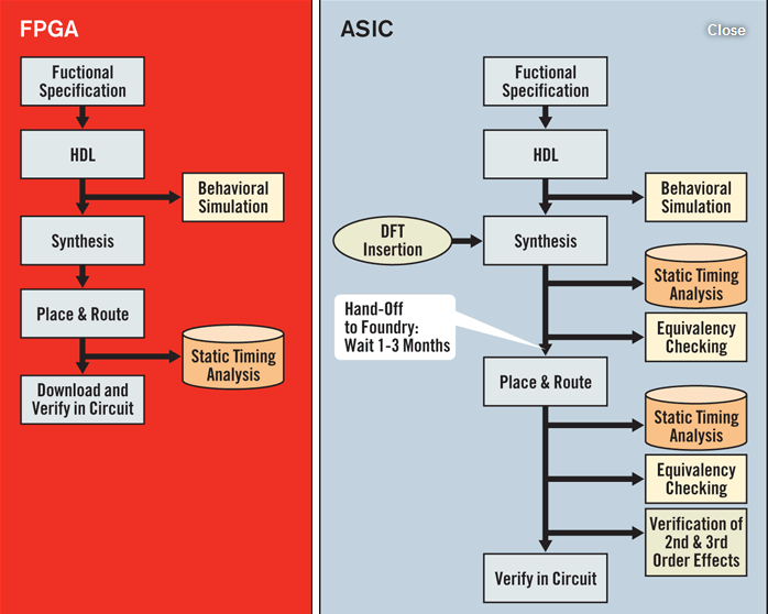
The implementation of ASICs is very costly but the overall unit cost covers up for the NRE cost and hence used only for mass production products. FPGA is a good option if the product is not in high numbers. Their production cycle also differ given by the image below.
An application-specific integrated circuit (ASIC /ˈeɪsɪk/) is an integrated circuit (IC) customized for a particular use, rather than intended for general-purpose use. For example, a chip designed to run in a digital voice recorder or a high-efficiency bitcoin miner is an ASIC.
Application-specific standard products (ASSPs) are intermediate between ASICs and industry standard integrated circuits like the 7400 series or the 4000 series.
As feature sizes have shrunk and design tools improved over the years, the maximum complexity (and hence functionality) possible in an ASIC has grown from 5,000 logic gates to over 100 million. Modern ASICs often include entire microprocessors, memory blocks including ROM, RAM, EEPROM, flash memory and other large building blocks. Such an ASIC is often termed a SoC (system-on-chip). Designers of digital ASICs often use a hardware description language (HDL), such as Verilog or VHDL, to describe the functionality of ASICs.
Since ASICs are custom circuits, they are very fast and use less power than an FPGA. This can be critical in power-sensitive applications such as cell phones, mp3 players, and other battery-operated devices.
The biggest drawback to an ASIC is cost. To get a company to build an ASIC for you will cost hundreds of thousands of dollars as an initial investment!
Reasons to use ASICs
- Size: An ASIC is obviously smaller than multiple interconnected standard products on a PC board. Having a variability in size allows the chip to be as small or as large as necessary. This reason alone is why many electronics are shrinking in size in recent years.
- Power and Performance: Because of their small physical size, ASIC devices can use far less electrical power as compared to a collection of standard components. In addition, an ASIC contains only the circuitry needed for the application, therefore, the chip is much more efficient due to the miniature size and power requirements.
- IP Protection: In addition to size, power and performance, ASIC chips provide you with IP protection, unlike a standard product. The chips specific to you. This means that it is much easier to differentiate yourself from the competition, and it also creates a very high barrier to entry.
- Competitive Edge: Although an initial investment is required to develop an ASIC, the payoff for this investment is very high. Aside from a possible performance enhancement, a product using an ASIC requires fewer electronic components and is much cheaper to assemble. Having fewer parts translates into higher reliability overall. An ASIC can house many different systems on a single chip, therefore, you will be reaching out to far less vendors when looking to assemble your final product. This means there will be less purchasing and production planning for products with many parts.
- Smarter, Faster, More Reliable: In the end, an ASIC is a smart choice for a variety of reasons. An ASIC can shrink your product’s size, costs can be considerably less, and you will have a chip that no one else has access to besides you. These reasons alone should give you enough incentive to consider development of your own ASIC. Sigenics, Inc. offers a very nifty ASIC cost calculator tool to help you assess financials behind your design and needs.
Some manufacturers offer multi-project wafers (MPW) as a method of obtaining low cost prototypes. Often called shuttles, these MPW, containing several designs, run at regular, scheduled intervals on a “cut and go” basis, usually with very little liability on the part of the manufacturer. The contract involves the assembly and packaging of a handful of devices. The service usually involves the supply of a physical design database (i.e. masking information or pattern generation (PG) tape). The manufacturer is often referred to as a “silicon foundry” due to the low involvement it has in the process.
ASIC stands for Application Specific Integrated Circuit. An ASIC is similar in theory to an FPGA, with the exception that it is fabricated as a custom
[See the full post at: What is ASIC and the difference between FPGA and ASIC]
What is ASIC and the difference between FPGA and ASIC
Related posts:
Related posts: